RZ/G Hardware Peripherals
← RZ-G
DDR
PCB Design and Verification Flow
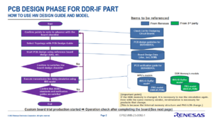
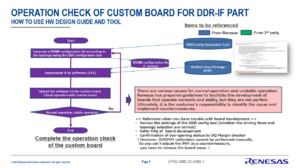
- Below is the recommended PCB Design and Verification Flow for DDR Interfaces.
- PDF Version (English/日本語) : File:DDR-IF PCB Design Verification Flow r1.0.PDF
DDR (auto) refresh and self-refresh
There is often a confusion between DDR auto refresh and self refresh, this small note is meant to shed some light on these two terms.
DDR refresh or auto refresh is simply the command that is sent from the DDR controller (DDRC) to the DDR chip periodically (in the range of milliseconds) to refresh the DDR content. This happens while normal operation, so all the signals including the clock are active.
DDR self-refresh instead is a low power mode that is entered by issuing the (auto) refresh command and keeping the CKE low. In this case the DDR chip uses an internal counter to trigger the refresh. In self refresh mode all the DDRC signals but CKE are "don't care" and they may not even be actively driven to save power.
In some cases, especially for DDR used in temperature sensitive applications, there is a feature called Auto Self-Refresh (ASR) that is basically an self-refresh with a variable refresh time automatically computed based on the temperature. If ASR is not supported normally the refresh time should be configured before the self-refresh mode is entered.
In RZ/G2 (E-N-M-H) there is a low power mode where all the power supplies but the DDRC I/Os (mainly to drive CKE) are off, to better support the so called suspend-to-RAM, that allows to keep the DDR content and save power. When the power supplies are back the MPU will reboot quicker by restoring its state from the one saved in the DDR before entering the low power mode. Obviously, in order for the suspend-to-RAM to be supported and all the power supplies off, there should be a PMIC that supports it and some software routines that handles the handshake, as well as the shutdown / wake up.
DDR test routines
There are a couple of "hidden" commands in the RZ/G2 flash writer that may be very useful during the bring-up of a custom board:
- DDRCK
- RAMCK start_address end_address
It would be a good idea to run these checks to ensure that the DDR is working fine.
Parallel display interface
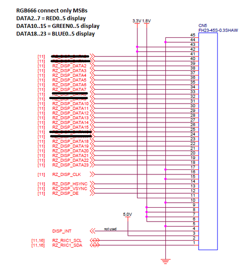
The parallel display interface is still supported by many RZ/G2 devices. This section is meant to clarify how to connect the display pins properly to be able to interface both RGB888 and RGB666 LCDs. Often there is a parallel to LVDS bridge in between but the same considerations apply.
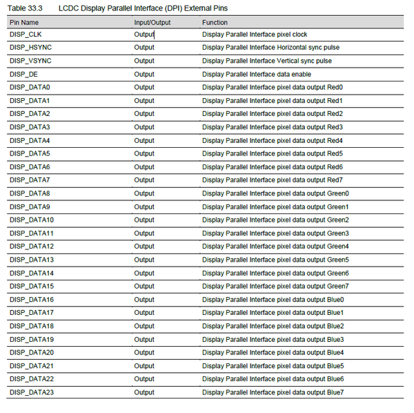
The parallel display interface normally includes data pins and control pins, e.g. VSYNCH, HSYNCH, pixel clock, etc. Different devices may have different names, in case of RZ/G2L-V2L-G2UL the pins names are quite generic: DISP_DATA0..23, so you may wonder how to connect them. However table 33.3 of the Users' Manual provides more details about the signals:
In case of RZ/G2E-N-M-H, the name of the data pin itself is self explaining: DU_R0..7, DU_G0..7 and DU_B0..7, where obviously R, G and B stand for Red, Green and Blue respectively.
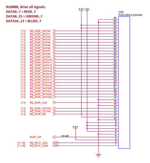
If your goal is to drive a RGB666 LCD, you may be thinking of using a lower color depth also for the framebuffers. However in MPU applications where there is usually a DDR as main volatile memory saving a couple of megabytes is not that important and sometimes not even possible. For example in RZ/G2L-V2L-G2UL the 18-bit per pixel formats use 4 bytes per pixel anyway. This simplifies the configuration, the only difference is in the HW. For RGB888:
For RGB666, the LSB color signals shall not be connected:
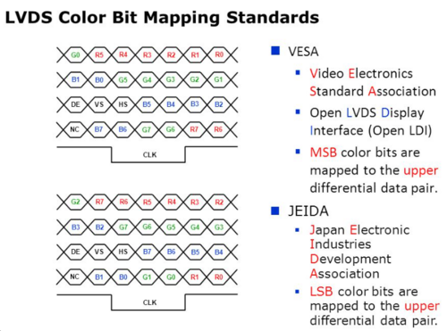
When it comes to parallel -> LVDS bridges, there are two main formats supported by LCDs: VESA and JEIDA. The main difference is that the first is used by displays expecting the two most significant bits of each color to be transferred over the 4th serial data output, whereas the latter the two least significant bits of each color to be transferred over the 4th serial data output.
The JEIDA format is very convenient for switching from 24-bits to 18-bits, basically it is enough to leave the 4th serial data output pair disconnected.
From the MPU point of view it is very important to choose the right connection (VESA or JEIDA) depending on the final LCD display: it is not possible to switch from one format to another, i.e. it is not possible to remap the color data position in SW, so pay particular attention to this.
Clock
RZ/G2L Main Clock
- RZ/G2L strictly needs only one 24MHz crystal.
- If Gigabit ethernet is used, then the transceiver typically needs a 25MHz clock, many are ok with a 25MHz quartz.
Audio Clock
As far as audio is concerned, in low cost applications the idea is to use another widely available clock in the system (e.g. 12MHz) and feed this into the codec that then acts as a master and feeds the audio clock back in into the MPU.
Power
RZ/G2L Power
- RZ/G2L needs 1.1V (most of the logic), 1.8V/3.3V IOs and other, 2.5V ethernet, 1.2V/1.35V DDR4/DDR3L respectively. 5V is not really required but most of the time also present.
- Realistic current requirements for main rails (1.1V, 1.2V, 1.8V, 3.3V) can be found in the reference power / thermal management documents.
eMMC
eMMC boot for RZ/G2E-N-M-H
There are some points to take in account regarding eMMC boot:
- RZ/G2N,M,H can only boot from MMC1 (aka SDHI3).
- Therefore, on the HiHope board, eMMC is connected to MMC1 and eMMC Boot can be performed.
- The IO voltage must be 1.8V for eMMC Boot.
Camera
MIPI-CSI2 virtual channels in RZ/G2
As per MIPI CSI-2 specification, each MIPI-CS2 interface can carry up to 4 virtual channels, each channel can be a video stream.
A bridge chip example is MAX9286.
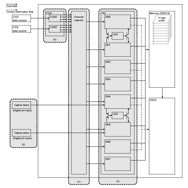
In the RZ/G2M, RZ/G2N and RZ/G2H there are 2 CSI-interfaces, CSI40 (4-lane) and CSI20 (2-lane), the maximum transfer rate is 1.5Gbit/s per lane. The total bandwidth results in a limitation in terms of maximum size video format, both for a single channel and for the 4 potential channels.
Each virtual channel can then be assigned to a VIN (Video Input Module) channel, that stores in memory the video data. VIN max capture size is 4096x4096 .
On top of MIPI-CSI2, in the RZ/G2M-N-H there are 2 digital inputs (parallel) that share 2 VIN channels with MIPI-CSI2:
Even if similar, the RZ/G2E is a bit different because it has less HW resources, both in terms of MIPI CSI-2 (one 2-lane CSI40 despite the name and one parallel input) and VIN (2 channels).
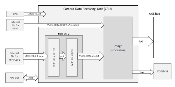
In case of RZ/G2L-LC-UL, the CRU (Camera Data Receiving Unit) is used instead of VIN. There's a single CRU instance and only one video stream can be stored in memory at a time. Depending on the target frame rate it would be technically possible to switch from the different virtual channels to capture different frames of different streams. The parallel input can also be used but it is mutually exclusive with MIPI.
| Product | Supported resolution(1) (up to) | Simultaneous input(s) (up to) | MIPI VC | Inputs |
|---|---|---|---|---|
| RZ/G2H, RZ/G2M, RZG2N | 4K | 8 | 4 | 2x MIPI-CSI2, 2x Parallel (RGB/YCbCr) |
| RZ/G2E | FHD | 2 | 2 | 1x MIPI-CSI2, 1x Parallel (RGB/YCbCr) |
| RZ/G2L | FHD | 1 | 4 | 1x MIPI-CS2, 1x Parallel |
| RZ/G2LC, UL | FHD (no codec) | 1 | 4 | 1x MIPI-CSI2 |
(1) This is not the maximum image size that can be captured, it is the highest resolution that can be displayed and / or encoded.


